Working Between the Schematic and the Board | Altium Designer 18.1 User

Altium 23 Create Multiple Page Pdf Schematic

Altium researcher Working between the schematic and the board

Schematic altium pdk ops mismatch document between devzone specification sheet nordic Managing design changes between the schematic & the pcb in altium Altium how to make it to follow net connection order..

Managing Design Changes between the Schematic & the PCB in Altium

1 (schematic circuit using altium designer 2017) source: researcher

Altium pcb routing reverse managing changes howie modified

Schematic mismatch between ops document and pdk schematicPower tips: simplify creation of multiphase and multimodular board Altium documentationAltium schematic connection follow order make pcb wires here schematics.

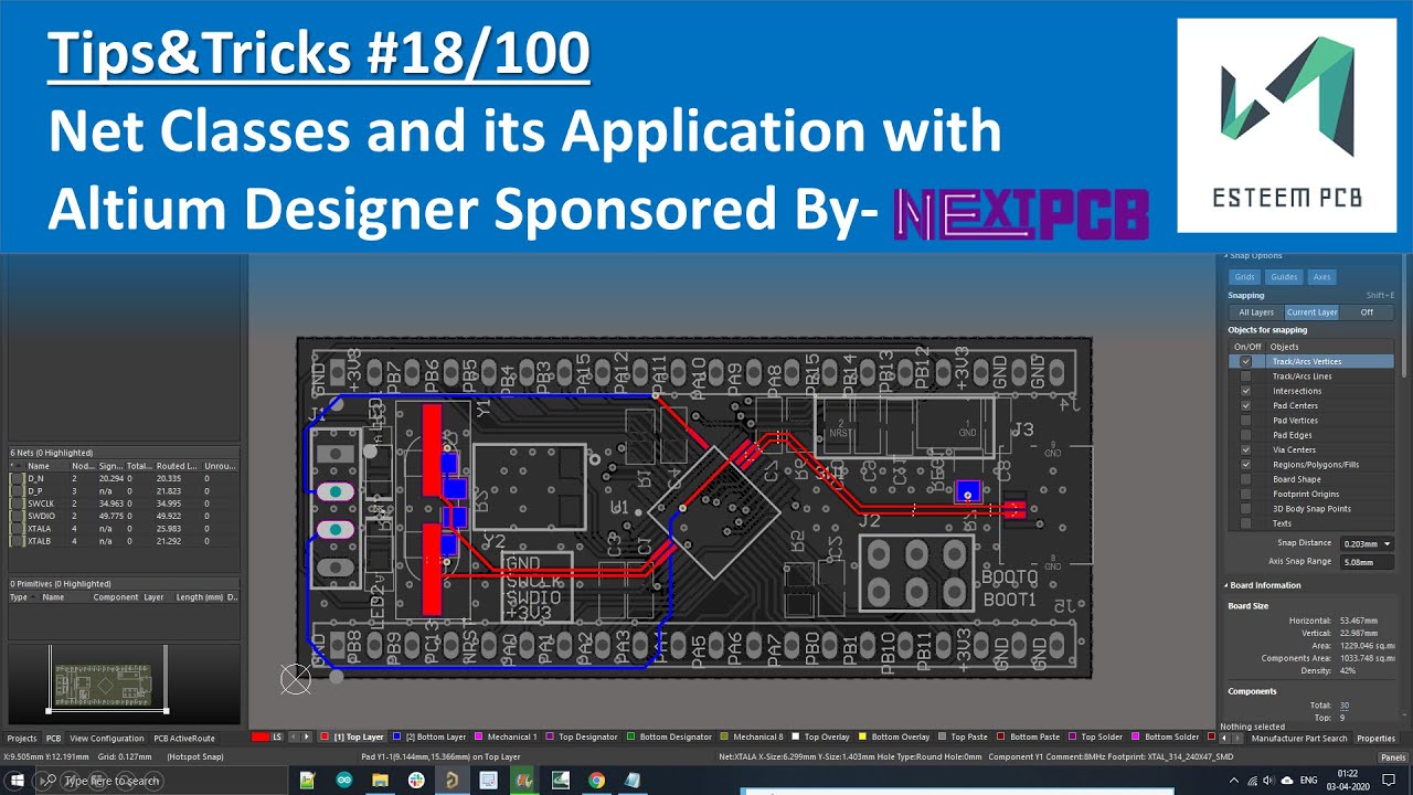
Altium designer tips #18: how to create net class in altiumAltium e2e multiphase simplify .

Altium how to make it to follow net connection order.. - Page 1
Altium Designer Tips #18: How to Create Net Class in Altium - YouTube
Power Tips: Simplify creation of multiphase and multimodular board
1 (Schematic Circuit using Altium Designer 2017) Source: Researcher
Working Between the Schematic and the Board | Altium Designer 18.1 User
Schematic mismatch between OPS document and PDK schematic - Nordic Q&A
Managing Design Changes between the Schematic & the PCB in Altium